
Views: 0 Author: Site Editor Publish Time: 2026-08-30 Origin: Site


Electronic products demand highly specialized packaging solutions. They must perfectly bridge two opposing forces. First, they require rigorous physical and environmental protection. Sensitive components need shielding from static shock, impact, and moisture infiltration. Second, they demand high retail visibility. Consumers consistently want to see the physical product before making a purchase decision. The stakes remain incredibly high for electronics brands. Selecting the wrong packaging configuration causes severe downstream issues. It leads directly to increased defect rates from electrostatic discharge or transit damage. It compromises retail security through easy pilferage on store shelves. Furthermore, poorly optimized designs inflate shipping weights unnecessarily.
You need a comprehensive strategy to avoid these costly pitfalls. This guide provides a clear technical and commercial framework. You will learn how to evaluate material properties, structural designs, and manufacturing capabilities. We will help you finalize your ideal packaging strategy confidently.
Every successful packaging project begins with a rigorous assessment of the product itself. You cannot apply a one-size-fits-all approach to electronic components. A delicate printed circuit board requires entirely different protection than a ruggedized charging cable. Establishing your core requirements early prevents costly redesigns during the manufacturing phase.
Understanding these three parameters ensures you select the optimal electronics blister packaging for your specific use case.
Once you define your core requirements, you must select a structural mechanism. The structural type dictates the unboxing experience, the security level, and the assembly speed. Each format offers distinct advantages and specific limitations.
Face seal configurations represent the most traditional approach. The mechanism involves a thermoformed plastic cavity heat-sealed directly to a coated cardboard backing. This style works best for low-cost consumer electronics, basic cables, and lightweight accessories.
The primary advantage lies in production speed and low tooling costs. Manufacturers produce these rapidly in massive volumes. However, face seal packaging carries notable trade-offs. It remains highly susceptible to tampering. Thieves can easily slice the cardboard backing or peel the plastic away. Therefore, avoid this style for high-value merchandise.
Trap blister designs offer a clever hybrid approach. The mechanism traps the plastic blister between two pieces of die-cut cardboard. The plastic never adheres directly to the board via heat sealing. Instead, the two cardboard cards seal to each other.
This format appeals heavily to modern brands. It prioritizes a sustainable unboxing experience. Consumers can easily separate the plastic from the cardboard for recycling. Furthermore, it provides enhanced graphic space. You get two full sides of cardboard for branding and instructions without sacrificing product visibility.
Clamshells provide the ultimate physical security. The mechanism features a hinged, one-piece enclosure. It folds over and snaps securely shut. Many brands choose to permanently ultrasonic-seal the edges for retail security.
These enclosures work best for heavy-duty applications. High-value consumer tech heavily relies on them. They also serve perfectly as hardware blister packaging, easily supporting the weight of heavy metal tools or dense battery packs. They deter pilferage effectively, though they require more plastic material than face seal alternatives.
Packaging Structural Types Comparison
| Structural Type | Primary Mechanism | Best Applications | Security Level |
|---|---|---|---|
| Face Seal Blister | Plastic sealed to a single backer card. | Low-cost cables, lightweight accessories. | Low (Prone to tampering) |
| Trap Blister | Plastic sandwiched between two cards. | Eco-conscious brands, mid-tier electronics. | Medium (Better structural integrity) |
| Clamshell | Hinged, fully enclosed plastic shell. | High-value tech, heavy hardware. | High (Especially when ultrasonically sealed) |
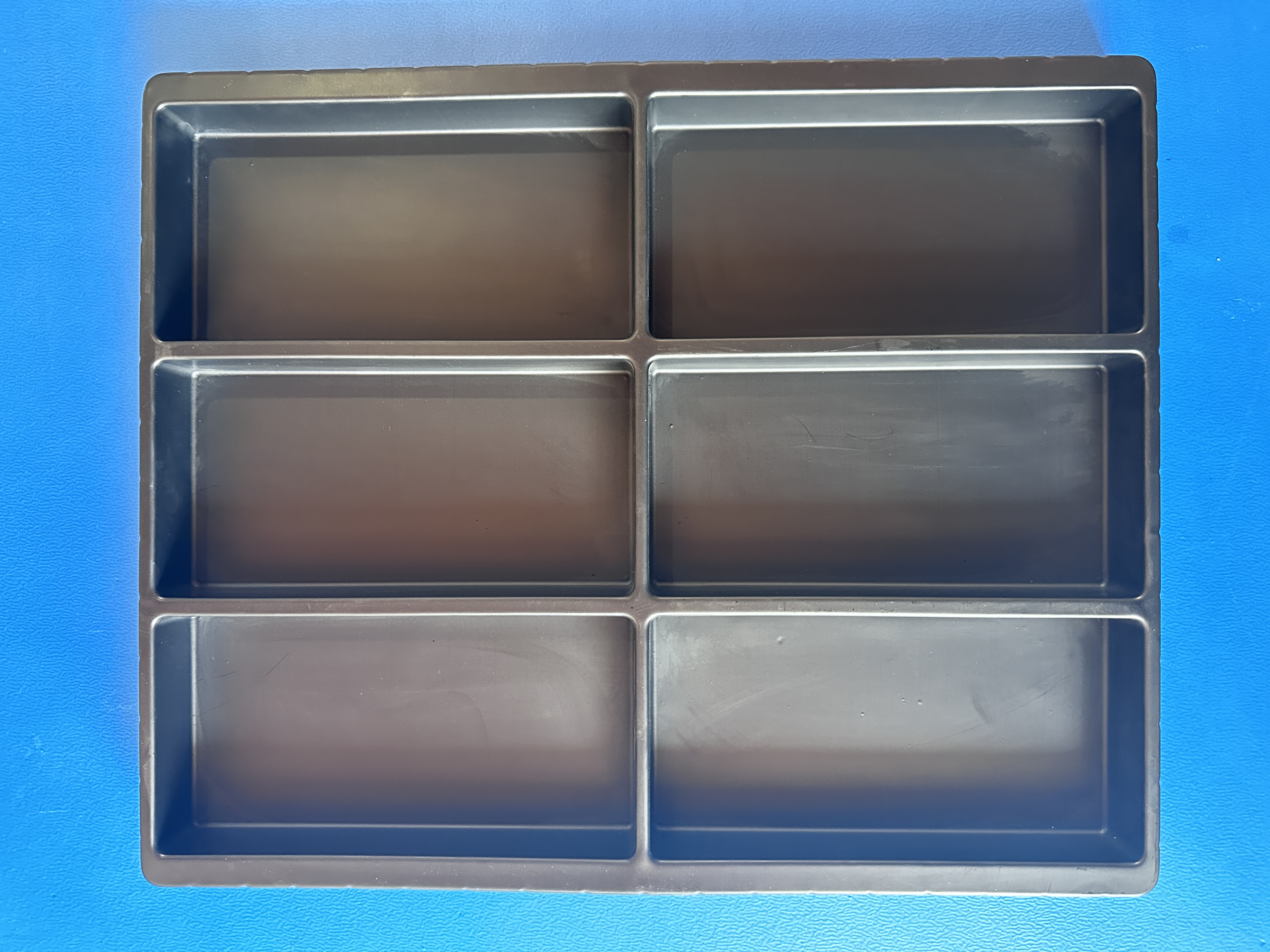
Material science plays a critical role in electronics packaging. You cannot evaluate plastic purely on cost. You must consider chemical properties, environmental compliance, and static behavior. The wrong resin choice can ruin an entire production run of sensitive devices.
Polystyrene holds a unique position in electronic manufacturing. We frequently thermoform it into specialized ESD trays and protective handling blisters. Manufacturers can treat or extrude polystyrene to become highly conductive or static-dissipative.
This material safely drains static charges away from delicate microprocessors. Using custom ps blister packaging ensures your components survive assembly line handling. However, it possesses a notable limitation. PS offers much lower optical clarity than alternative plastics. It often appears cloudy or opaque black. Consequently, engineers use it primarily when physical and electrical protection heavily outweighs retail presentation needs.
Polyethylene Terephthalate dominates the retail electronics sector. It serves as the undisputed industry standard. PET delivers superior optical clarity, allowing consumers to inspect screens and connectors easily. It also boasts immense tensile strength, preventing cracks during transit.
More importantly, Recycled PET (RPET) satisfies modern environmental mandates. It allows brands to utilize post-consumer recycled content without compromising structural integrity. RPET easily forms into complex geometries, making it highly versatile for clamshells and trap blisters.
Historically, PVC ruled the packaging industry. It remains highly durable and extremely cost-effective. Many legacy hardware brands still utilize it for heavy tools. However, modern electronics brands actively phase it out.
PVC presents significant environmental compliance issues. It releases harmful toxins during production and disposal. Strict frameworks like RoHS and REACH increasingly restrict its use in the European Union and other major markets. You should actively avoid PVC if you plan to distribute your electronic products globally.
Moving from a conceptual design to a mass-produced reality requires precise engineering. Vague dimensions lead to assembly line jams and shipping failures. You must lock in exact parameters before cutting any production-grade tooling.
You must carefully engineer the internal cavity holding the product. The cavity design must allow for easy de-nesting. When trays stack tightly together for shipping, they often stick. Proper draft angles (the slight taper applied to vertical walls) prevent this vacuum effect. Furthermore, generous tolerances ensure automated robotic arms can load parts seamlessly. Tight cavities put unnecessary friction stress on delicate electronic pins, glass screens, or fragile connectors during insertion.
You must establish the minimum mil-thickness required for your specific product weight. Thin plastics warp under pressure. You want to prevent corner-crushing during palletization. A heavy power adapter might require a 30-mil thickness, while a simple USB drive survives perfectly in a 12-mil cavity. Proper thickness testing guarantees the packaging retains its shape throughout the entire supply chain journey.
If you use face seal or trap blisters, you must outline strict sealing metrics. Specify the exact heat-seal coatings required on your cardboard cards. Document the necessary dwell times (how long the press holds down) and operating temperatures. These metrics must remain perfectly compatible with your contract packager’s existing automated machinery. Mismatched sealing parameters cause cards to curl or blisters to fall off in transit.
Never assume a design works without physical validation. Mandate standardized drop-test protocols, such as ISTA (International Safe Transit Association) standards. These tests simulate brutal shipping environments. Additionally, verify total material compliance. Ensure your selected plastics avoid banned substances, guaranteeing smooth customs clearance for international shipping. Defining comprehensive electronics blister packaging specifications upfront eliminates expensive manufacturing revisions later.
Your packaging is only as reliable as the manufacturer producing it. A brilliant CAD design fails if the factory cannot hold tight production tolerances. Vetting your partners thoroughly removes massive risk from your product launch.
Evaluate their engineering department first. Does the supplier offer rapid prototyping? Top-tier manufacturers utilize CNC machining or industrial 3D printing to create proof-of-concept molds. You should always receive a physical prototype before they cut the final, production-grade aluminum tooling. This step allows you to test the physical fit of your electronic device, ensuring the snap-fits engage correctly and the draft angles perform as intended.
Request documentation regarding their internal QA procedures. Look for current ISO certifications. A reliable partner implements documented processes for measuring material distribution. During thermoforming, plastic stretches as it pulls into deep cavities. Poor manufacturing controls cause severe wall thinning, creating weak spots in the packaging corners. Your supplier must measure and guarantee uniform thickness across every batch.
Finally, assess their material sourcing network carefully. The global plastics market frequently experiences severe resin shortages. Ask potential partners about their raw material redundancy. Do they rely on a single local distributor, or do they hold direct relationships with multiple global resin extruders? A resilient electronics blister packaging supplier ensures your production lines keep moving, even during global supply chain disruptions.
Optimal electronics packaging requires a delicate balancing act. You must carefully weigh static and physical protection against retail presentation needs and budget constraints. Choosing the correct structural type and material directly influences your product's market success. Avoid outdated materials like PVC, and embrace scalable designs like trap blisters or RPET clamshells for future-proof compliance.
Your immediate next steps are clear. Draft a preliminary requirements document outlining your product's exact weight, ESD sensitivity, and anticipated production volume. Reach out to shortlisted manufacturers. Request physical material samples and detailed tooling quotes. By approaching the selection process methodically, you guarantee a secure, attractive, and highly functional packaging solution for your electronics.
A: Anti-static materials prevent the initial buildup of triboelectric charges caused by friction. Static-dissipative materials go a step further. They allow existing electrical charges to flow slowly and safely to a grounded surface. Your choice depends entirely on the specific voltage sensitivity of your PCB or electronic component.
A: Costs vary drastically by design complexity. Simple face seal molds generally cost much less than intricate, multi-cavity clamshell molds. However, investing in inexpensive rapid prototyping molds first can mitigate the massive risk of costly errors before you purchase full-production aluminum tooling.
A: Yes, absolutely. You can achieve this by utilizing RPET (recycled PET) to incorporate post-consumer waste. Alternatively, transitioning to trap blister designs significantly reduces the total plastic-to-cardboard ratio. This improves overall sustainability while maintaining the rigorous structural integrity needed for heavy hardware.
A: The timeline typically spans 3 to 6 weeks from initial CAD design approval to first-article production. This duration heavily depends on the supplier's in-house tooling capacity and the complexity of the thermoforming mold required for your specific product.


